Any links to online stores should be assumed to be affiliates. The company or PR agency provides all or most review samples. They have no control over my content, and I provide my honest opinion.
The widely rumoured Samsung Exynos 9825 chipset has been announced ahead of the Galaxy Note10 later today.
Unlike the Snapdragon 855 refresh with the 855 Plus, the Exynos 9825 is a bit more than just a clock bump. The new Exynos 9825 SoC is now manufactured on the Samsung 7nm LPP (EUV) fabrication process which should bring a range of advantages.
The Exynos Galaxy S10 was criticised by many reviewers for its poor battery life compared to the SD855 variation, one reason for this is that the SD855 is made on 7nm silicon from TSMC vs the 8nm of Samsung’s. As well as the power disadvantages, this also means that the die area was physically larger on the Exynos at 127mm² versus the smaller 73mm² competition.
So, in theory, the Snapdragon 855/855+ and Exynos 9825 should now be level pegging in terms of power efficiency from the fabrication process, though other factors will affect this.
On top of the improved fabrication process, Samsung has bumped up their core clocks similar to the Qualcomm, at the moment it is unclear on how the GPU is affected, but the two Cortex A75 cores have gone from 2.31 GHz to 2.4 GHz which represents a 3.9% improvement.
In comparison the Snapdragon 855 Plus raised the clocks of the Prime CPU core by 120Mhz from 2.84GHz to up to 2.96GHz, giving a 4.2% boost. So it will be interesting to see how the increase in frequency across the middle, not top cores, will affect the Samsung performance.
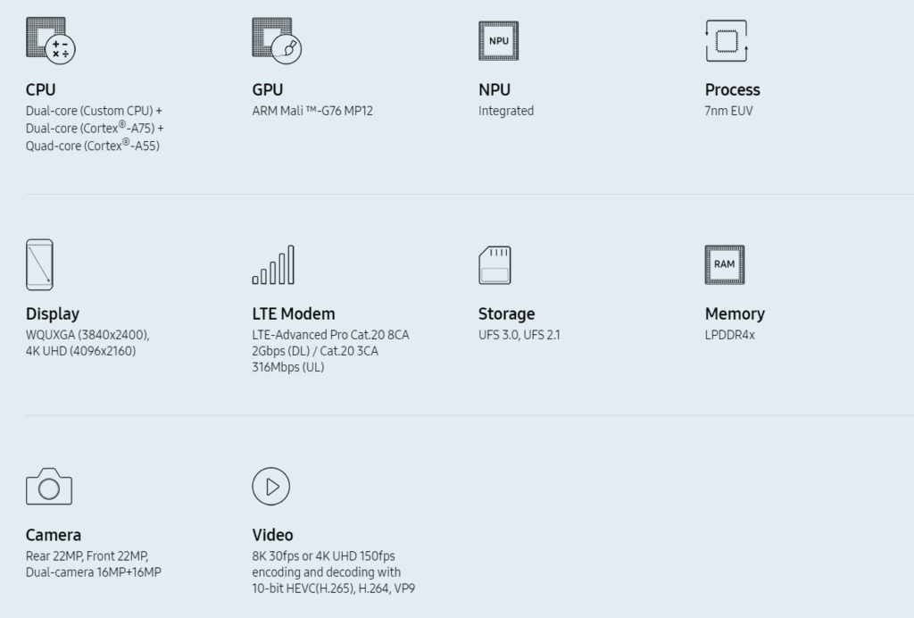
On the GPU side, Samsung has also stuck with the same GPU configuration as with 9820, using a MP12 configuration of the Mali G76. According to the company, the 9825’s GPU is clocked higher – so it will outperform its predecessor, however, the company has yet to disclose specific clock speeds.
Qualcomm raised their GPU clocks by 87Mhz from 585MHz to 672MHz which represented a 15% improvement, so I wouldn’t be surprised to see a similar increase here.
Previously there were rumours that the new Note10 would feature the Snapdragon 855 Plus but it now looks like this is not the case and the Exynos 9825 SoC will allow them to have performance parity or better than the SD855+.
| Exynos 9825 | Exynos 9820 | Snapdragon 855+ | |
|---|---|---|---|
| Process | 7nm LPP (EUV) | 8 nm LPP (Low Power Plus) FinFET | 7nm (N7) |
| CPU Cores | Octa-Core, 64-bit | Octa-Core, 64-bit | Octa-Core, 64-bit |
| CPU | 2x M4 @ 2.73 GHz 2x Cortex A75 @ 2.4 GHz ? 4x Cortex A55 @ 1.95 GHz ? | 2x M4 @ 2.73 GHz 2x Cortex A75 @ 2.31 GHz 4x Cortex A55 @ 1.95 GHz | 1x Kryo 485 Gold (A76 derivative) @ 2.96GHz 1x512KB pL2 3x Kryo 485 Gold (A76 derivative) @ 2.42GHz 3x256KB pL2 4x Kryo 485 Silver (A55 derivative) @ 1.80GHz 4x128KB pL2 2MB sL3 |
| GPU | Mali G76MP12 @ ? MHz | Mali G76MP12 @ 702 MHz | Adreno 640 @ ~672MHz |
| NPU | Yes | Yes | Yes (Hexagon 690 DSP) |
| RAM | 4x 16-bit CH LPDDR4X @ 2093MHz | 4x 16-bit CH LPDDR4X @ 2093MHz | 4x 16-bit CH @ 2133MHz LPDDR4x 34.1GB/s 3MB system level cache |
| ISP | Rear: 22MP Front: 22MP Dual: 16MP+16MP | Rear: 22MP Front: 22MP Dual: 16MP+16MP | Dual 14-bit Spectra 380 ISP 1x 48MP or 2x 22MP |
| Video Playback & Codecs | 8K30 & 4K150 encode & decode H.265/HEVC, H.264, VP9 | 8K30 & 4K150 encode & decode H.265/HEVC, H.264, VP9 | 2160p60 10-bit H.265 HDR10, HDR10+, HLG 720p480 |
| Modem | Shannon 5000 Integrated LTE (Category 20/13) DL = 2000 Mbps 8x20MHz CA, 256-QAM UL = 316 Mbps 3x20MHz CA, 256-QAM | Shannon 5000 Integrated LTE (Category 20/13) DL = 2000 Mbps 8x20MHz CA, 256-QAM UL = 316 Mbps 3x20MHz CA, 256-QAM | Support for WiFi 6 standard (802.11ax) as well as the new 60GHz “Wi-Gig” 802.11ay, enabled by an external WiFi combo chipset. |
| Charging | Samsung Adaptive Fast Charge, Fast Wireless Charging (Qi & PMA) | Samsung Adaptive Fast Charge, Fast Wireless Charging (Qi & PMA) | Quick Charge 4+ (USB PD Compatible) |
I am James, a UK-based tech enthusiast and the Editor and Owner of Mighty Gadget, which I’ve proudly run since 2007. Passionate about all things technology, my expertise spans from computers and networking to mobile, wearables, and smart home devices.
As a fitness fanatic who loves running and cycling, I also have a keen interest in fitness-related technology, and I take every opportunity to cover this niche on my blog. My diverse interests allow me to bring a unique perspective to tech blogging, merging lifestyle, fitness, and the latest tech trends.
In my academic pursuits, I earned a BSc in Information Systems Design from UCLAN, before advancing my learning with a Master’s Degree in Computing. This advanced study also included Cisco CCNA accreditation, further demonstrating my commitment to understanding and staying ahead of the technology curve.
I’m proud to share that Vuelio has consistently ranked Mighty Gadget as one of the top technology blogs in the UK. With my dedication to technology and drive to share my insights, I aim to continue providing my readers with engaging and informative content.

